
When you’re shipping components worth more than some startups, every detail matters. The semiconductor equipment industry runs on purity, precision, and zero tolerance for error. WIC Packaging provides engineered packaging solutions for the machines and components that build the world’s most advanced tech. We help clients navigate complex logistical and environmental challenges, including:
Cleanroom Care. Warehouse Tough.
Supply Chain Solutions for the Semiconductor Industry.

Preventing electrostatic discharge (ESD) during transport

Meeting cleanroom compliance and avoiding contamination

Handling ultra-fragile and high-value components

Managing the removal and relocation of legacy fab equipment
Designing packaging for oversized or non-standard machinery
Safeguarding against corrosion and foreign object debris (FOD)
Solutions Designed for the Most Demanding Tech
From prototype wafers to room-sized UV systems, we protect critical semiconductor equipment at every stage—from first shipment to final upgrade. Our packaging systems are custom-built for purity, structural integrity, and regulatory compliance.
- ESD-safe barrier bags and vacuum-sealed protection
- Cleanroom-ready packaging materials and processes
- Desiccant-integrated systems for moisture and corrosion control
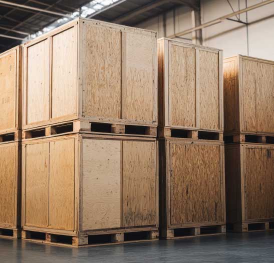
- Oversized crate design for heavy and complex machinery
- On-site packaging and crate assembly inside or near fab facilities
- Rigging coordination with trusted partners for fab removals and installs

Engineered for the Semiconductor Supply Chain
Our teams don’t just design packaging. We show up where it counts. From secure global shipment to on-site fab prep, WIC Packaging delivers hands-on solutions and specialized services for the semiconductor sector, including:
- On-site packaging teams embedded in customer facilities
- Custom crates for large-format and irregularly shaped equipment
- ESD audits and best-practice packaging consulting
- Cleanroom packaging for internal process components
- Prototype wafer packaging for new product development
- FOD-free packaging for clean-critical applications
News

Ship Shape: How to Choose the Right Partner for Semiconductor Packaging
Ship Shape: How to Choose the Right Partner for Semiconductor Packaging
Read More
The Many Forms of Foam: Part One
The Many Forms of Foam: Part One
Read More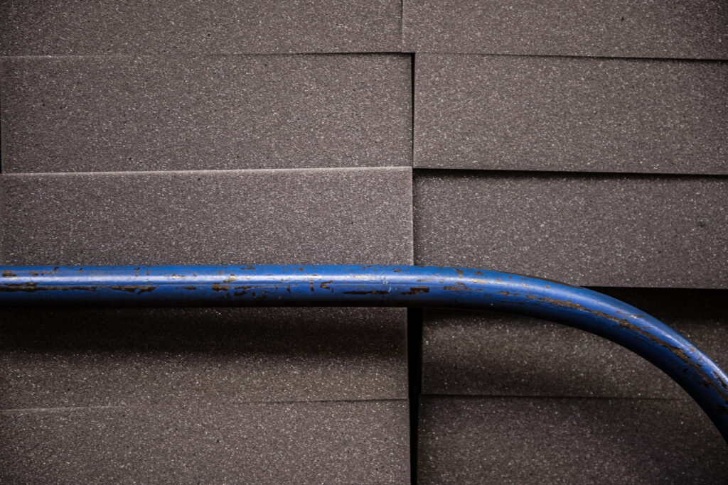
The Many Forms of Foam: Part Two
